60 GHz 3D IC TSV–Micro-Bump–RDL Interconnect Modeling and Signal Integrity in HFSS 2024 R2
Investigate high-frequency interconnect behavior in a 3D IC transition comprising through-silicon vias, micro-bumps and redistribution-layer routes up to 60 GHz.
Research objective
Investigate high-frequency interconnect behavior in a 3D IC transition comprising through-silicon vias, micro-bumps and redistribution-layer routes up to 60 GHz.
Software and model scope
Primary environment: ANSYS HFSS 2024 R2. Discipline: Electronics, VLSI and RF Engineering. The video provides a project demonstration; source models, solver settings and plots should be checked against the actual implementation before reuse.
Simulation / modelling methodology
- Construct a grounded stack-up with explicitly defined TSV barrels, dielectric liners, micro-bumps, RDL traces and reference conductors.
- Assign conductor properties and dielectric loss parameters appropriate for the stated frequency range.
- Configure wave/lumped terminals or differential ports consistently and validate port references before sweeping.
- Extract S-parameters, inspect return loss, insertion loss, crosstalk and discontinuities while checking mesh convergence.
Outputs and checks for validation
- Insertion loss and return loss through 60 GHz
- Near-end/far-end crosstalk for multiport models where ports exist
- Current distribution and electric-field hot spots at transition discontinuities
- Optional eye-diagram/BER estimates from separately documented channel post-processing
How to interpret results
S-parameters describe a linear channel, not an automatically computed PAM4 eye or BER. Accurate eye/BER analysis requires transmitter/receiver, equalization and channel-processing assumptions.
Verification caveat: Check differential vs single-ended port definitions, conductor roughness, dielectric properties, mesh settings and whether an observed resonance belongs to the interconnect or a port/fixture artifact.
Applications for OEM and PhD research
Chiplet interconnects, heterogeneous packaging, high-speed chip-to-chip links, TSV/RDL optimization and signal-integrity research.
Project thumbnail
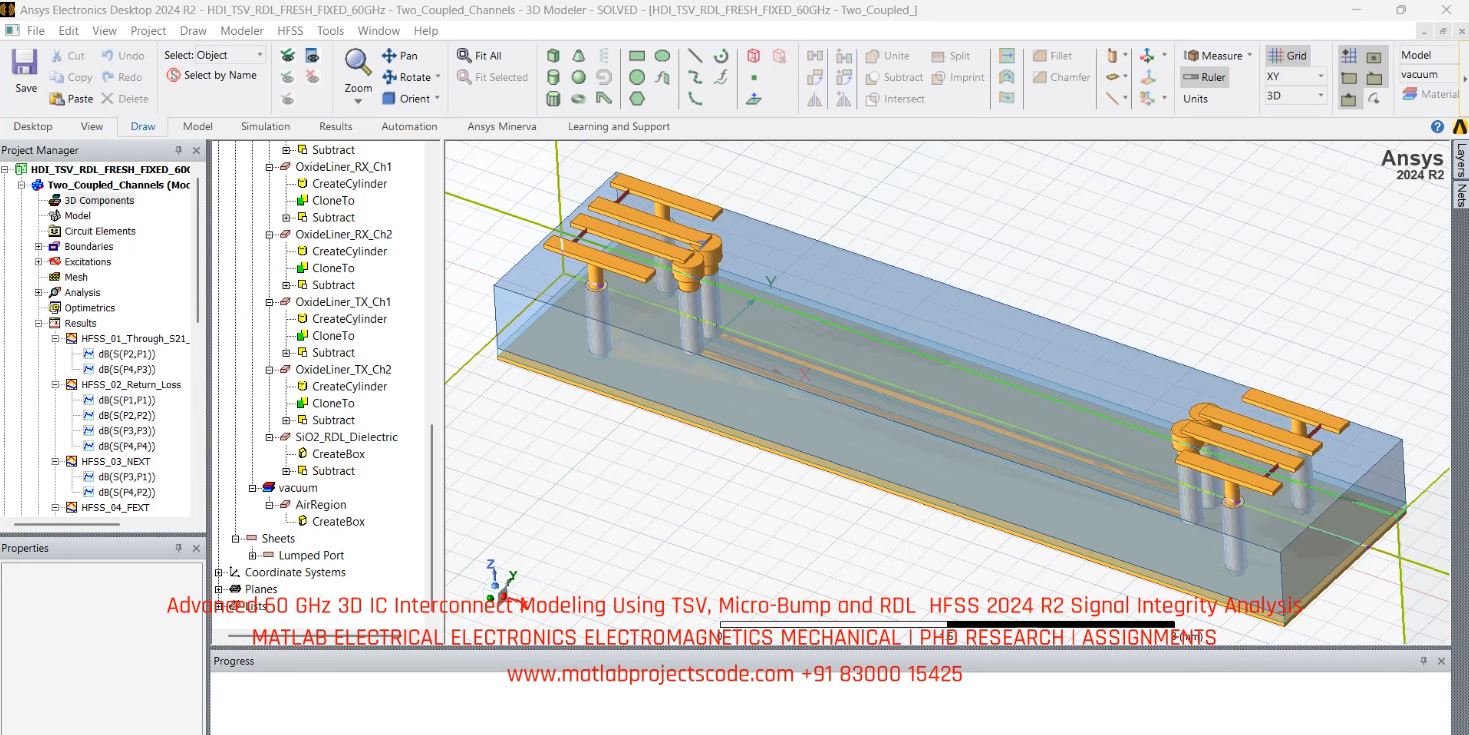
Preview image is matched to the hosted file after media synchronization.
Frequently asked questions
Which software is used for this simulation?
ANSYS HFSS 2024 R2 is the primary environment named in this project.
What should be checked before using its results?
Check differential vs single-ended port definitions, conductor roughness, dielectric properties, mesh settings and whether an observed resonance belongs to the interconnect or a port/fixture artifact.
Can this project support a new research comparison?
It can serve as a reference workflow, but any new claim requires a fresh model, documented parameters, independent validation and genuinely measured outputs.
Important notice
contents are for representative purposes, actual content may vary
OEM / PhD Research Enquiry
Request the model scope, software requirements, validation plan and expected deliverables for this topic.
Contact the simulation team WhatsApp +91 83000 15425