An Electrical Model for Nanometer CMOS Device Stress Effect in Design and Simulation of Analog Refer
An Electrical Model for Nanometer CMOS Device Stress Effect in Design and Simulation of Analog Refer project page for MATLAB/Simulink simulation, OEM prototyping…
PROJECT_OBJECTIVE
An Electrical Model for Nanometer CMOS Device Stress Effect in Design and Simulation of Analog Refer is prepared as a dedicated Mechanical, EV and Mechatronics Engineering simulation project page for OEM teams, PhD research scholars, engineering students and research laboratories in AU, UK, CA and global markets.
SOFTWARE_USED_AND_MODEL_SCOPE
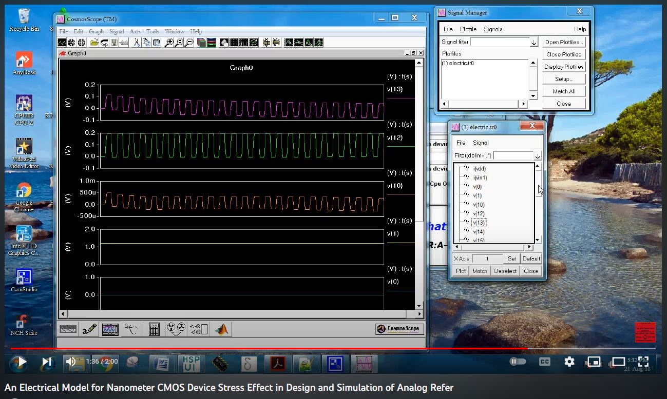
Software used: MATLAB/Simulink. The model can include source files, parameters, subsystem screenshots, controller logic, waveform outputs and technical documentation.
Simulation model explanation: system modelling, parameter setup, controller or algorithm implementation, simulation runs and interpretation of measurable outputs for academic and OEM validation.
CONTROL_ALGORITHM_METHODOLOGY
The methodology can be expanded with mathematical modelling, block-level signal flow, controller/algorithm design, assumptions, solver settings, parameter tuning and comparison cases for An Electrical Model for Nanometer CMOS Device Stress Effect in Design and Simulation of Analog Refer.
EXPECTED_WAVEFORM_OUTPUTS
- simulation response plots
- parameter table
- model screenshots
- result explanation
APPLICATIONS_AND_RESULT_INTERPRETATION
Applications include academic implementation, PhD proof-of-concept modelling, journal validation, OEM prototype assessment, controller comparison, result reproduction and engineering documentation. Result interpretation can explain waveform behaviour, transient response, steady-state performance and domain-specific output quality.
VIDEO_TRANSCRIPT_AND_THUMBNAIL
This video preview demonstrates the An Electrical Model for Nanometer CMOS Device Stress Effect in Design and Simulation of Analog Refer simulation workflow for Mechanical, EV and Mechatronics Engineering. It helps OEM engineers, PhD scholars and research teams review the model structure, key input parameters, output response and validation path in MATLAB/Simulink.
Direct video file for search engines: open MP4 simulation output.
PROJECT_FAQ
What is the objective of An Electrical Model for Nanometer CMOS Device Stress Effect in Design and Simulation of Analog Refer?
The objective is to model, simulate and explain An Electrical Model for Nanometer CMOS Device Stress Effect in Design and Simulation of Analog Refer as a research-ready Mechanical, EV and Mechatronics Engineering workflow with verifiable outputs for OEM evaluation, PhD research and engineering documentation.
Which software is used for An Electrical Model for Nanometer CMOS Device Stress Effect in Design and Simulation of Analog Refer?
The project is prepared around MATLAB/Simulink and can be supported with model files, simulation setup, parameter values, output graphs and explanation notes.
Can this project be modified for a thesis or journal paper?
Yes. The model can be customized for new parameters, control algorithms, comparison tables, waveform style, university formatting and journal-style methodology sections.
What files can be delivered for this project?
Delivery can include the source model, simulation video reference, screenshots, graphs, parameter sheets, report documentation and a detailed explanation of the result interpretation.
REPRESENTATIVE_CONTENT_NOTICE
Notice: contents are for representative purposes, actual content may vary according to the final source model, software version, parameter settings, waveform requirements, report format and OEM or PhD research customization.